High Energy Accelerator Research Organization (KEK)
Japan Science and Technology Agency (JST)
Executive summary
Question
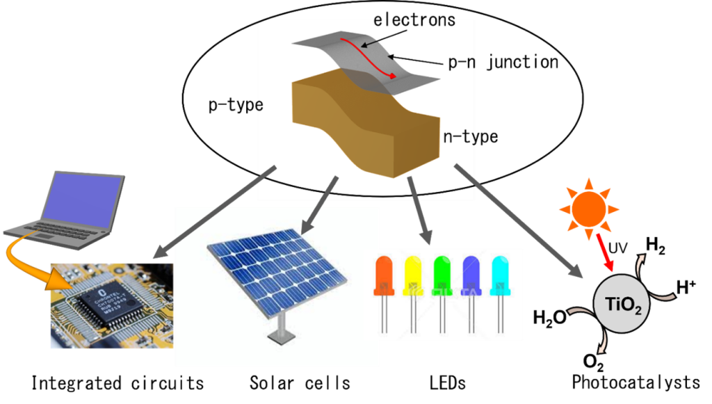
The p-n junction interface, at which p-type and n-type semiconductors are bonded plays a central role in semiconductor devices. It was discovered about 70 years ago;however, up to date, the p-n junction interface has not been directly observed.
Findings
By further developing the experimental setup created by Fukumoto (one of the authors of the manuscript) that can visualize conductive electrons in semiconductors, we succeeded in observing the real and energy-spaces of the charge-depleted region formed at the p-n junction interface.
Meaning
This method enables the evaluation of semiconductor devices by direct visualization. It is applicable to all semiconductor devices, and hence is expected to contribute to the development of the semiconductor industry.
Overview
Using a photoemission electron microscope with a femtosecond pulsed laser light source (fs-PEEM) (※1) installed at the Institute of Materials Structure Science (IMSS), High Energy Accelerator Research Organization (KEK), we succeeded in imaging the shape of the depletion layer (※2), which is formed at the semiconductor p-n junction interface and plays an important role in controlling electric current, during device operation. This new method is expected to be used to characterize various semiconductor devices such as diodes, transistors, solar cells, and LEDs, as it can visualize the internal state of the device while evaluating its performance.
※1.fs-PEEM
A microscope in which the sample is irradiated by photons and the emitted photoelectrons are detected (Figure 2). By using an ultrashort pulse laser as the light source, the photon energy can be freely varied in the near-infrared, visible, and ultraviolet light ranges. This makes it possible to efficiently observe conductive electrons.
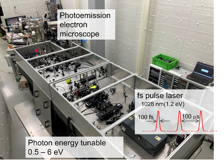
The laser pulses are extremely short, with each pulse irradiating the sample for only 100 fs (1 femtosecond is one millionth of 1 billionth of a second), and a gap of 100 microseconds (1 microsecond is one millionth of a second) between the pulses.
※2.Depletion layer
When a p-type semiconductor and an n-type semiconductor are bonded, the energy levels at the interface are inclined so that the energy levels of the valence band of the p-type semiconductor, where holes are the majority charge carriers, and the conduction band of the n-type semiconductor, where electrons are the majority charge carriers are aligned. This creates a region (depletion layer) where electrons and holes do not exist. In a normal diode, when an external voltage is applied in the forward direction, the inclination becomes smaller and charges flow. In the reverse direction, the inclination becomes larger and no current flows. In a tunnel diode, electrons move from the valence band of the p-type semiconductor to the conduction band of the n-type semiconductor by applying a reverse bias voltage so that they tunnel through the depletion layer.
Please refer to the press release for details.
Contacts
High Energy Accelerator Research Organization (KEK) Public Relations Office
e-mail: press@kek.jp