KEK物質構造科学研究所 構造生物学研究センター研究員の長瀬里沙さん。幼少のころからバレエひとすじでしたが、25歳の時に転機が訪れ、胃がん研究の研究者に転身しました。全く違うジャンルへの転身のきっかけは何だったのか?ご本人にお聞きしました。
―長瀬さんは研究者になる前はバレエをされていたそうですね。
「3歳ごろからバレエをやっていて、バレエをするのが当たり前だったので、『将来は当然仕事にするだろう』と思っていました。高校を卒業してから、子どもにバレエを教えながらバレエ教室に所属していました」
―バレリーナだった長瀬さんが胃がんの研究を始めようとされたきっかけは?
「25歳のころ、遺伝子の変異でがんになるというがんを特集したテレビ番組を見たことがきっかけです。叔父が12歳の時、伯母は40歳の時に胃がんで亡くなり、ほかにも胃がんの手術をするなど胃がんを発症することの多い家系で、『原因を明らかにしてそれを予防することができれば』という思いが沸きあがりました」
―そこから勉強をはじめられたのですか?
「高校を卒業してからずっとバレエをしていたので、まずは大学受験の勉強からでした。自分でもびっくりするくらいできなくて(笑)食事の時以外は勉強、という生活でした。26歳で神奈川大学の生物科学科に入学しました。自分で『やろう』と決めたからできたことですね」
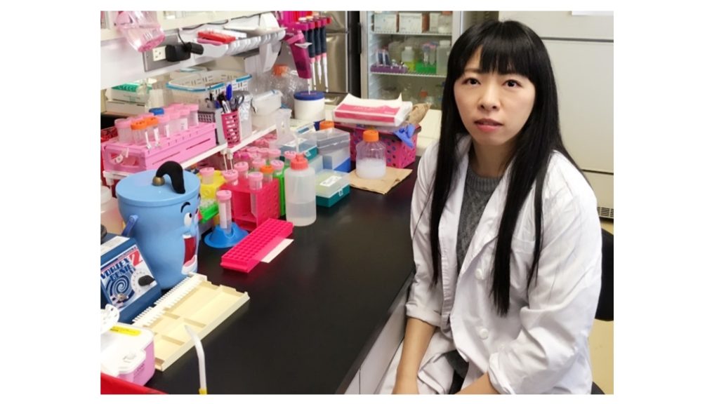
―KEKにはいつからいらっしゃるのですか?
「大学卒業後、北海道大で修士号を取り、その後東京大学の医学系研究科で4年かけて博士号を取得しました。そのまま東大で研究員をしていて、2015年7月にKEKの研究員になりました」
―KEKでの研究の内容は?
「胃がんの原因の研究をしています。ピロリ菌が産生する CagA というたんぱく質は胃の上皮細胞にあるたんぱく質 SHP2 と結びつくことで胃がんの発症を促すと考えられています。そこで私は、X線結晶構造解析という技術を利用して詳細な立体構造情報を得ることで、CagA と SHP2 がどのように結合しているのかを明らかにするという研究しています」
―研究成果はどういったことに活用できそうですか?
「CagA と SHP2 が結合しなければがんにならないのでは、と考えられるので、この結合を防ぐ薬剤の開発などにつながればと思います」
―研究のやりがいはどういうところですか?
「基本的には実験室など室内で一人で行う仕事なので、論文を出してそれに対する反応があると社会とつながっていると思えて、次また頑張ろうと思います。研究はトライアル・アンド・エラーの繰り返しなので、日々継続しなければ上昇していけないバレエで培った忍耐力が今役に立っていると思います。まるで違う世界と思って始めましたが、意外と役に立つ部分があるなと思います」
―「やりたい」という思いが原動力ですね。
「自分がやりたいと思ったことであれば、知らず知らずのうちにできるようになっていることが多いし、結果的に成功できるのだと思います。研究者は、誰も知らないことを自分が明らかにすることができる、とても夢のある仕事ですね。毎日楽しいと思える仕事が得られているのはとても幸運だと思います」
(聞き手:広報室 牧野佐千子)